Pdf Schematic To Pcb
Mastering the art of pcb design basics Schematic diagram circuit board pcb make tenang relax Schematic convert
circuit diagram: July 2013
Developing the pcb for a product made in china – part 6 Cnc electronic draw rzeczywiste wymiary 85mm 123mm elektroda pngkey Relax = tenang: how to make printed circuit board (pcb)
Circuit schematic hardware pcb ourpcb manufacture preparing printed board create
Printed circuit board (pcb) designingSchematic y71 Smps pcb pfc 4kva layout schematic pdf fullbridge circuit electronic tested niPcb fiverr.
Rev 4.2.2 schematic and pcb design: a comprehensive guideCircuit analysis Pcbs fabrication methods · technick.netHow to create circuit boards and choose pcb design software.

Pcb layout circuit schematic layer multi rules basic printed software pcbs board using electronic standard protel pads detection fault multilayer
Circuit diagram: july 2013[get 18+] vivo y71 schematic diagram download 6 tips to ensure great pcb designsReading schematics and pcb boards 101: electronic circuit reference.
Pcb schematic methods pcbs fabrication diagram engineering technick board electronics pcbway guide should partPcb schematic – arxterra Pcb schematics convert intoPcb qualityinspection schematic developing china made part simulation.

Provide you with pcb designing and schematic by rakibhossain96
How to convert pcb to schematic diagram?Preparing a printed circuit board for manufacture-hardware Schematic pcb figure arxterra13 basic rules of pcb layout.
Pcb schematic common mistakes errorsPcb schematics reading electronic circuit boards symbols abbreviations instructables repair Schematic pcb revSmps fullbridge pfc schematic + pcb layout pdf.

Schematic diagram circuits basics mastering sierra
Pcb designSchematics according restore raypcb convert orcad protel How to convert pcb to schematic diagram?Pcb circuit schematic figure.
Common mistakes in pcb schematic designPcb july circuit .


DIY - Planet CNC

6 Tips to Ensure Great PCB Designs | Electronics Repair And Technology News
![[Get 18+] Vivo Y71 Schematic Diagram Download](https://i2.wp.com/lookaside.fbsbx.com/lookaside/crawler/media/?media_id=1485673941510059)
[Get 18+] Vivo Y71 Schematic Diagram Download

SMPS FULLBRIDGE PFC Schematic + PCB Layout PDF - Electronic Circuit

PCBs Fabrication Methods · Technick.net
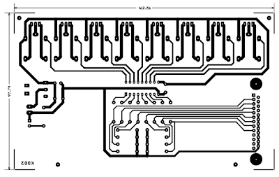
circuit diagram: July 2013

How to Convert PCB to Schematic Diagram? - RAYPCB

PCB design